Printed Circuit Board Assembly (PCBA) lies at the heart of modern electronics manufacturing. It is a complex process that transforms raw materials into functional circuit boards used in everything from smartphones to industrial machinery. This article delves into the stages and technologies involved in pcba manufacturing.
1. Design and Prototyping
PCBA manufacturing starts with the design phase. Engineers use specialized software to create the circuit board layout, determining the placement of components and routing of electrical connections. Once the design is finalized, a prototype board is produced for testing and validation.
2. Component Procurement
The next critical step is component procurement. Manufacturers source various electronic components such as resistors, capacitors, integrated circuits, and connectors from suppliers. These components are selected based on specifications, quality, and availability to ensure they meet the design requirements.
3. PCB Fabrication
Simultaneously, the printed circuit board itself is fabricated. This involves several key steps:
- Substrate Preparation: A substrate material (typically fiberglass-reinforced epoxy laminate) is chosen based on the board’s requirements.
- Layering: Multiple layers of substrate are sandwiched together to create the required number of conductive layers.
- Etching: Copper is selectively removed from the substrate to create the circuit pattern using chemical etching or a subtractive process.
- Drilling: Holes are drilled for component mounting and electrical connections.
- Surface Finishing: The exposed copper surfaces are coated to prevent oxidation and ensure solderability.
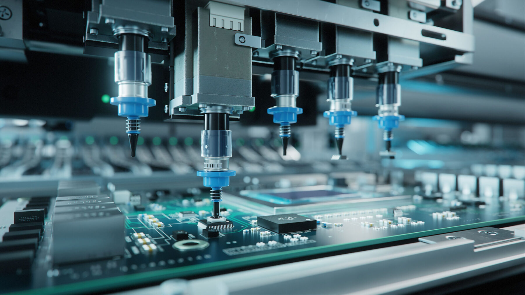
4. SMT Assembly
Surface Mount Technology (SMT) is the most common assembly technique used in PCBA manufacturing. This process involves:
- Stencil Printing: Solder paste is applied to the PCB through a stencil, depositing it onto the pads of the board.
- Component Placement: Automated machines place surface-mount components (like resistors and ICs) onto the PCB accurately.
- Reflow Soldering: The PCB is heated in a reflow oven, melting the solder paste and creating strong electrical connections.
5. Through-Hole Assembly (PTH)
For components that cannot be surface-mounted, like connectors and large capacitors, Through-Hole Technology (THT) is used. This involves:
- Manual or Automated Insertion: Components are manually or automatically inserted into pre-drilled holes on the PCB.
- Wave Soldering: The PCB is passed over a wave of molten solder, which secures the components to the board.
6. Inspection and Testing
Quality control is crucial throughout the manufacturing process. PCBA undergoes several inspections:
- Automated Optical Inspection (AOI): Machines check for defects in soldering, component placement, and alignment.
- Functional Testing: Boards are powered up and tested to ensure they function as intended.
- In-Circuit Testing (ICT): Test points are probed to verify electrical continuity and component functionality.
7. Cleaning and Coating
Once assembly and testing are complete, the PCBs are cleaned to remove flux residues and other contaminants. Some PCBs may also be conformal coated to protect them from environmental factors such as moisture and dust.
8. Packaging and Shipping
Finally, the finished PCBAs are packaged according to customer specifications and shipped to their destinations, ready for integration into the final electronic products.
PCBA manufacturing is a highly specialized process that combines precision engineering with advanced automation. From initial design to final assembly, every step is critical to producing reliable and efficient circuit boards.